ADC board
Introduction
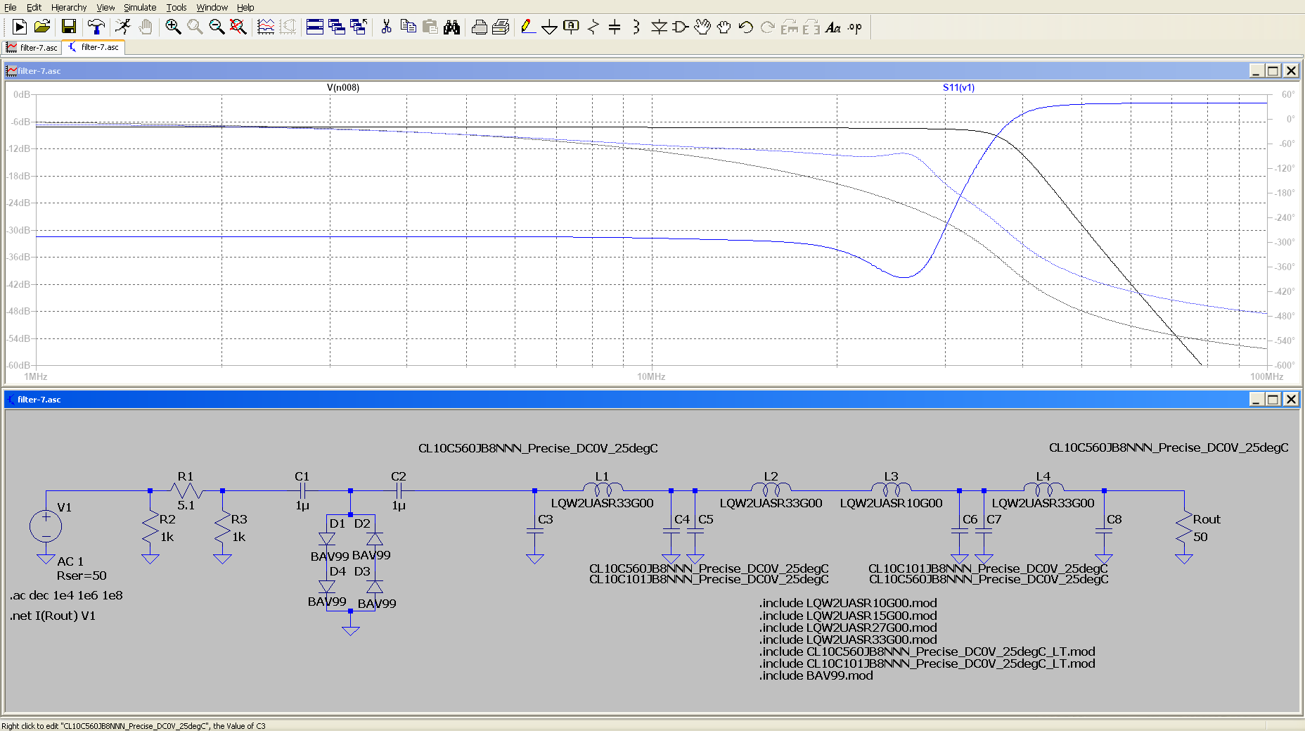
The ADC board is based on the AD9255-80 ADC. The sample rate is 77.76 MSPS. It has antenna input protection and a 30 MHz low-pass filter.
The KiCad files for the ADC board can be found in the qmtech-adc repository.
The ADC analog front-end is more or less as recommended by the ADC datasheet for frequencies below 50 MHz:

The antenna input protection circuit is similar to RF clipper with some improvements.
The 30 MHz low-pass filter uses 0805 2% capacitors and 1008 2% inductors available from JLCPCB.
The simulation results of the antenna input protection circuit and 30 MHz low-pass filter are shown in the following screenshot:
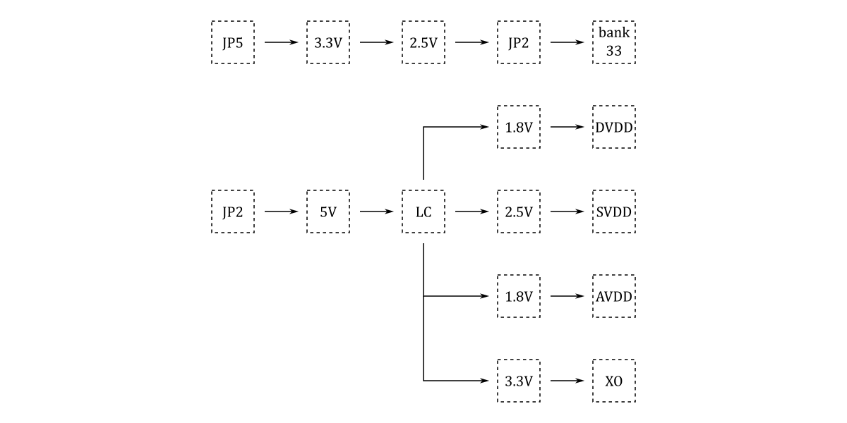
The FPGA bank 33 is externally powered with 2.5 V to enable the internal termination resistors for the LVDS inputs.
Separate linear regulators are used to power the DVDD, SVDD, AVDD and the oscillator.
The 5 V power input also contains a ferrite bead LC filter to filter out high frequency noise that linear regulators cannot filter.
The structure of the power subsystem is shown in the following diagram:
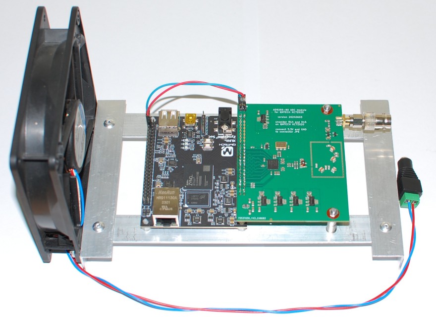
A 12 cm, 12 V, 1600 RPM low speed fan (e.g. Sunon HAC0251S4) can be used to cool both the QMTECH XC7Z020 board and the ADC board. It cools the boards well without an additional heatsink even when the fan is powered at low voltage (5 V). The platform that I use to support the boards and fan is shown in the following image:
Ordering ADC board from JLCPCB
Download and unpack the ADC board release zip file
Log in to jlcpcb.com
Click "Order now" at the top right of the web page
Click "Add gerber file" and provide the location of
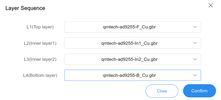
qmtech-ad9255.zipClick "Yes" in the "Specify Layer Sequence" section and specify layer sequence as shown in the following screenshot:
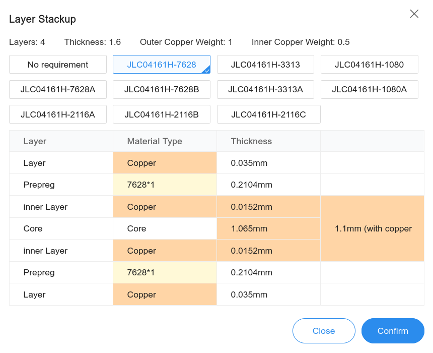
- Click "Yes" in the "Specify Stackup" section and specify layer stackup as shown in the following screenshot:
Enable "PCB Assembly"
Select 2 or 5 assembled boards in the "PCBA Qty" section
Click "Next"
Click "Next" on the "PCB" screen
Click "Add BOM file" and provide the location of
bom.csvClick "Add CPL file" and provide the location of
positions.csvClick "Process BOM & CPL"
Click "Next" on the "Bill of Materials" screen
If some parts are not available, then you will need to pre-order them before ordering the assembled ADC board
Click "Next" on the "Component Placements" screen
In the "Product Description" section select "Reserch\Education\DIY\Entertainment" and "Development Board - HS Code 847330"
Click "Save to cart"
Select "JLCPCB (PCB/PCBA/Stencil)" and click "Secure Checkout" on the "Shopping Cart" screen
Select the correct addresses, shipping and payment methods on the checkout screens
Connecting ADC board to QMTECH XC7Z020 board
Additional required connectors are listed at this link.
Resistors R14 and R15 should be unsoldered from the QMTECH XC7Z020 board.
Two 2x25 header strips should be soldered to the QMTECH XC7Z020 board.
One 2x25 socket strip should be soldered to the ADC board.
One 1x2 header strip should be soldered to the ADC board.
One SMA connector should be soldered to the ADC board.
The 2x25 socket strip on the ADC board should be connected to the extension connector JP2 on the QMTECH XC7Z020 board.
The 3.3V and GND pins of the 1x2 header strip on the ADC board should be connected with a double wire to the 3.3V and GND pins of the extension connector JP5 on the QMTECH XC7Z020 board.
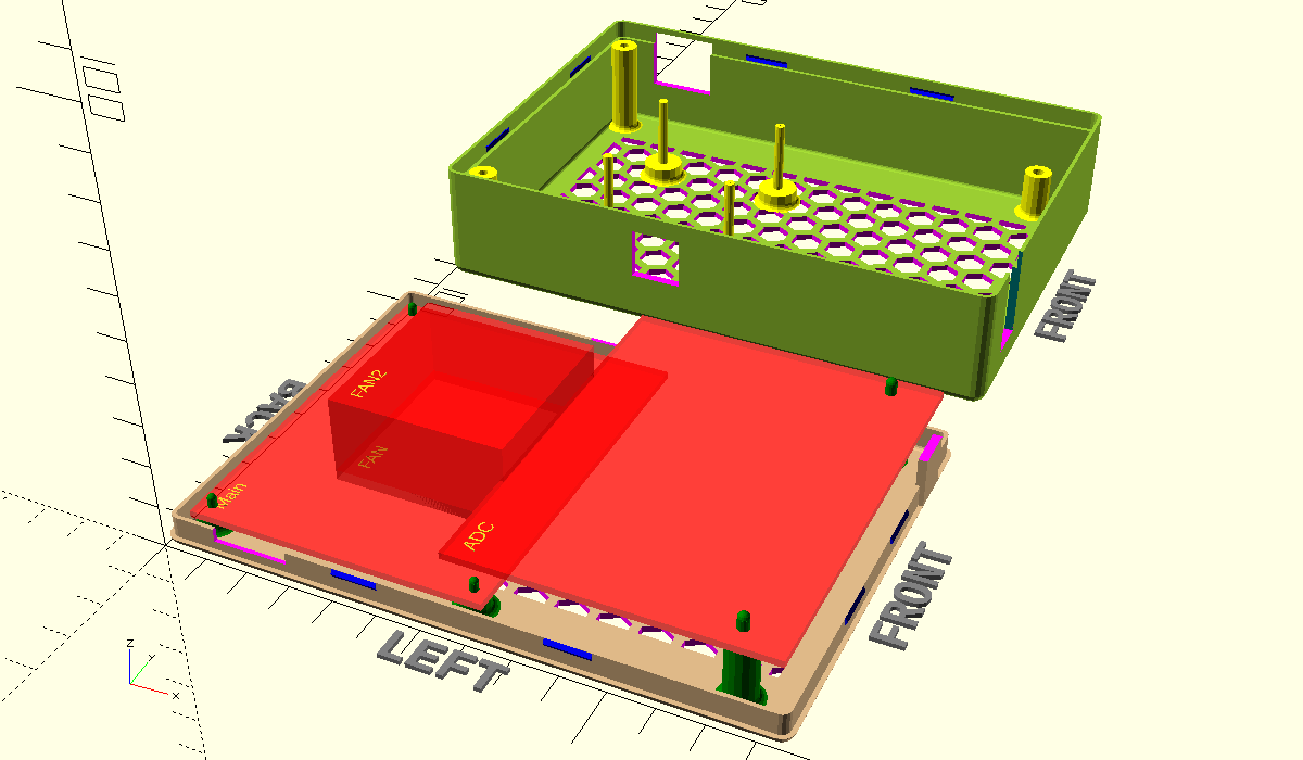
3D printable enclosure
This 3D printable enclosure is designed by Simon S53ZO using OpenSCAD and YAPP_Box.
The OpenSCAD files for this enclosure can be found in the qmtech-adc repository. These OpenSCAD files can be used to modify this enclosure.
A pre-built STL file can be found in the ADC board release zip file. This pre-built STL file can be used to print this enclosure with a 3D printer.
The two parts of this enclosure are shown in the following image: