Buffers for AXI4, AXI4-Lite and AXI4-Stream interfaces
Interesting links
Some interesting links on implementation of buffers and AXI4 interfaces:
Requirements
Since the AXI4 protocol specification requires that there are no combinational paths between input and output signals, it is useful to have reusable modules that would add the registers to the output signals of AXI4 interfaces.
To achieve good performance, these modules should have low resource usage and minimal latency.
Here are the main signals of the read address and read data parts of the AXI4 slave interface:
input  wire [ADDR_WIDTH-1:0] s_axi_araddr,  // AXI4-Lite slave: Read address
input  wire                  s_axi_arvalid, // AXI4-Lite slave: Read address valid
output wire                  s_axi_arready, // AXI4-Lite slave: Read address ready

output wire [DATA_WIDTH-1:0] s_axi_rdata,   // AXI4-Lite slave: Read data
output wire                  s_axi_rvalid,  // AXI4-Lite slave: Read data valid
input  wire                  s_axi_rready   // AXI4-Lite slave: Read data ready
In the read address part of the interface, the arready signal should have a register. In the read data part of the interface, the rdata and rvalid signals should have registers. So, two types of buffers are needed, one with one register on the data input side and one with two registers on the data output side as shown in the diagrams below:
If an interface buffer with registers on both sides is required, then these two types of buffers can be chained together to create such a buffer.
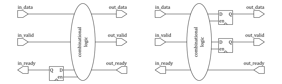
Input buffer
The in_ready signal of the input buffer should have a register and this buffer should have the following behavior:
in_readyregister is set to high during reset- when
in_readyis high,in_validandin_dataare directly connected toout_validandout_data - when
out_validis high andout_readyis low,in_readybecomes low,out_validandout_datashould output the last valid data untilout_readygoes high
A circuit implementing this behavior is shown in the following diagram:

The corresponding Verilog code can be found in modules/input_buffer.v.
Output buffer
The out_valid and out_data signals of the output buffer should have registers and these registers should be updated while out_ready is high or out_valid is low.
A circuit implementing this behavior is shown in the following diagram:

The corresponding Verilog code can be found in modules/output_buffer.v.
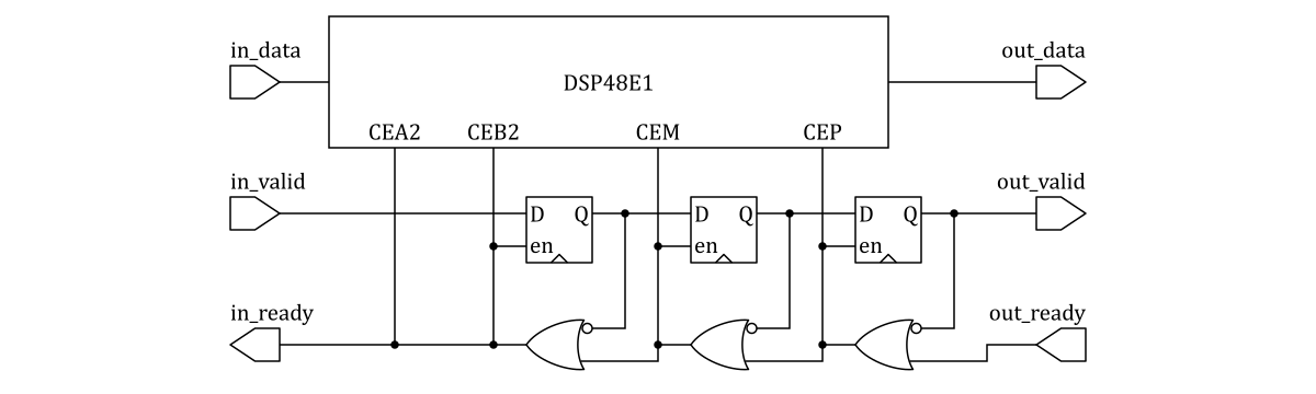
Since the in_ready signal is used to enable the data register, it can also be used to enable data registers outside the output buffer module. This feature can be useful when controlling a pipeline that provides enable inputs for its internal registers, like for example the internal registers in DSP48E1 as shown in the diagram below:
Usage examples
The Verilog code of the modules that use these input and output buffers can be found at the following links: